Electron Microscopy
The electron microscope uses a focused electron beam energized up to 106eV to provide images and chemical information with very high spatial resolution. Since the short wavelength of electron beam and the successful development of low aberration electron optical lenses, the atomic resolution is routinely achievable for transmission electron microscope (TEM), as well as the resolution close to 1 nanometer for scanning electron microscope (SEM). The SEMs collect secondary and back scattered electrons to imaging the surface area, called SEI and BEI, while the TEMs mainly use the transmitted signals of a thin specimen. With a scanning device attached, a TEM can perform both transmission and scanning microscopy. Electron diffraction patterns can be obtained from TEM simultaneously as well as electron channeling patterns for SEM. Chemical analysis with a finely focused beam is another advantage of electron microscopy, such as electron dispersive X-ray (EDX) analysis and electron energy loss spectroscopy (EELS). The newly developed high coherent source, field emission gun of single crystal tungsten, has made high-resolution imaging and microanalysis with a beam size less than 1nm for TEM and close to 1nm for SEM possible. Now the power of electron microscopy has been widely used in almost every field of materials research, since it can provide both surface and microstructural information and the microscopes are getting more computerized.
Scanning electron microscopes
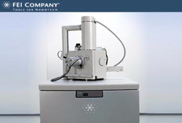
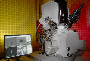
High resolution scanning electron microscope completely controlled under WindowNT. Equipped with a high stability Schottky field emission gun and a large specimen chamber (379x280 mm door si…

Scanning electron microscope completely controlled under WindowNT; currently equipped with tungsten tip for high beam currents; large specimen chamber (379x280 mm door size). Voltage: 200 -…
High resolution scanning electron microscope completely controlled under WindowNT. Equipped with a high stability Schottky field emission gun and a large specimen chamber (379x280 mm door si…
High resolution scanning electron microscope completely controlled under WindowNT. Equipped with a high stability Schottky field emission gun and a large specimen chamber (379x280 mm door si…
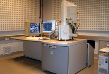
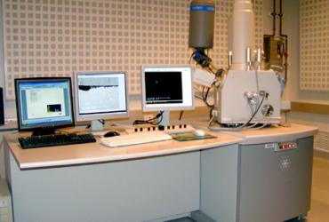
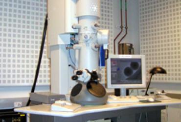
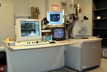
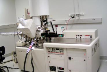
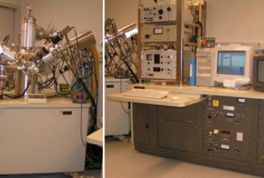
Transmission electron microscopes

This microscope is designed for 200kV and lower operation voltages, suitable for studies of biological, organic and other beam sensitive materials. For that purpose, this microscope is equip…
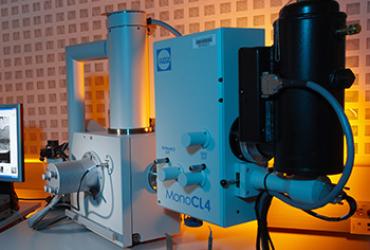
With a field emission gun (FEG), this microscope is designed for both high resolution TEM/STEM and analytical microscopy. The attachments of this microscope are: (1) A scanning unit with a h…
Scanning Probe Microscopy
The scanning probe microscope (SPM) operates exactly as its name implies: a sharp tip is scanning on sample surface in a controlled contact or non-contact mode, and the signals carrying surface information are collected, processed and then plotted on a computer screen. The first base of SPM was scanning tunneling microscope (STM) that was invented 1982. After that, it has also been found not only the tunneling current, but also the atomic force and other kinds of interactions in between tip and sample surface can be probed. Therefore, the category of SPM samples is greatly extended from conducting to non-conducting or soft materials since the tip can work just in a near-surface scan. The name of scanning probe microscopy summarizes scanning tunneling microscopy, atomic force microscopy (AFM), scanning capacitance microscopy (SCM), magnetic force microscopy (MFM) as well as a range of other measuring techniques.
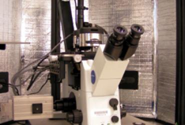
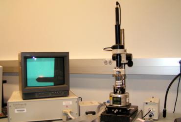
Scanning probe microscopes (STM/AFM)
Operation Modes: AC, Contact, LFM, Force, Nanolithography, EFM and Conductive AFM,…
Operation Modes: AC, Contact, LFM, Force, Nanolithography, EFM and Conductive AFM, and Low Force Indenter.
F…
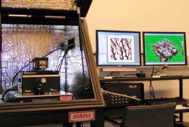
These SPMs have the similar functions in surface measurements with the Milti-Mode microscope as stated above. The major difference is that this microscope is designed for imaging a 6" wafer.…
This microscope can be performed at both tapping and contact mode with highest resolution manufactured. With either the D-type (10x10x25µm) or the J-type scanner (125x125x5µm), images on bot…
Surface Analysis Systems
Atom Probe Microscopes
Atom probe provides atomic -resolution, three-dimensional imaging, compositional imaging, and analyses. The Imago atom probe is used to analyze the structure and composition of materials for…
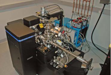
Focused Ion Beam Systems
DB235 is small stage system combining a Hexalens electron column and a Magnum ion column for failure analysis and high-end sample preparation. A Schottkey emitter is used for scanning electr…
The instrument is equipped with an Elstar field emission SEM for nanometer resolution imaging and a Tomahawk FIB column operating from 30kV down to 500V. Ion currents range from 7pA, providi…
X-ray Photoelectron Spectroscopy System
Purchased in 2001, the Kratos Ultra combines fast, high-sensitivity XPS (X-Ray Photoelectron Spectrometry) with a unique "real-time" imaging capability that allows us to quickly produce 2-di…
Secondary Ion Mass Spectrometry System
Dynamic SIMS is used for depth profiling solid materials, allowing a determination of elemental composition as a function of depth. The key attributes of SIMS are its unparalleled sensitivit…
Electron Microscopy Simulation
Electron simulation software are loaded into a Mac and two PC computers that are open to users. Location: 1429 CNSI
Electron Flight Simulator (PC)
"Electron Flight Simulation" (Version 3.1) by Small World, Inc.
Environmental SEM analysis simulation and modeling software for Windows.
More details: www.small-world.net